Elimination of the Impact of Trap Charges through Heterodielectric BOX in Nanoribbon FET

- Authors: Lakshmi Nivas Teja1, Rashi Chaudhary2, Shreyas Tiwari3, Rajesh Saha4
-
View Affiliations Hide Affiliations1 Department of Electronics and Communication Engineering, Malaviya National Institute of Technology Jaipur, Rajasthan 302017, India 2 Department of Electronics and Communication Engineering, Malaviya National Institute of Technology Jaipur, Rajasthan-302017, India 3 Department of Electronics and Communication Engineering, Malaviya National Institute of Technology Jaipur, Rajasthan-302017, India 4 Department of Electronics and Communication Engineering, Malaviya National Institute of Technology Jaipur, Rajasthan-302017, India
- Source: Nanoelectronic Devices and Applications , pp 231-245
- Publication Date: July 2024
- Language: English
Elimination of the Impact of Trap Charges through Heterodielectric BOX in Nanoribbon FET, Page 1 of 1
< Previous page | Next page > /docserver/preview/fulltext/9789815238242/chapter-12-1.gif
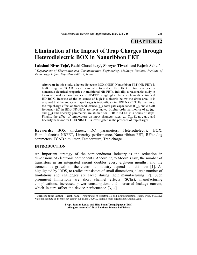
In this study, a heterodielectric BOX (HDB) Nanoribbon FET (NR-FET) is built using the TCAD device simulator to reduce the effect of trap charges on numerous electrical properties in traditional NR-FETs. Initially, a reasonable study in terms of transfer characteristics of NR-FET is highlighted between homodielectric and HD BOX. Because of the existence of high-k dielectric below the drain area, it is assumed that the impact of trap charges is insignificant in HDB NR-FET. Furthermore, the trap charge effect on transconductance (gm ), total gate capacitance (Cgg), and cut-off frequency (fc ) in HDB NR-FETs are investigated. Higher-order harmonics of gm (gm2 and gm3) and linearity parameters are studied for HDB NR-FET in a series of steps. Finally, the effect of temperature on input characteristics, gm , Cgg, fc , gm2, gm3, and linearity behavior for HDB NR-FET is investigated in the presence of trap charges.
-
From This Site
/content/books/9789815238242.chapter-12dcterms_subject,pub_keyword-contentType:Journal -contentType:Figure -contentType:Table -contentType:SupplementaryData105

