Synthesis and Characterization of CdS and ZnS Nanostructured Thin Films for Opto-electronic Energy Applications

- Authors: Raghavendra Bairy1, Vijeth H.2, Rajesh K.3, Rohan S. Deshmukh4
-
View Affiliations Hide Affiliations1 Department of Physics, NITTE (Deemed to be University), NMAM Institute of Technology, Nitte 574110, Karnataka, India 2 Department of Physics, School of Science, Nagaland University, Lumami 798627, Nagaland, India 3 Department of Physics, St. Joseph Engineering College, Mangaluru (Affiliated to VTU Belagavi) 575028, Karnataka, India 4 Department of Mechanical Engineering, Walchand College of Engineering, Vishrambag, Sangli 416415, MS, India
- Source: Thin Film Nanomaterials: Synthesis, Properties and Innovative Energy Applications , pp 1-35
- Publication Date: July 2024
- Language: English
Synthesis and Characterization of CdS and ZnS Nanostructured Thin Films for Opto-electronic Energy Applications, Page 1 of 1
< Previous page | Next page > /docserver/preview/fulltext/9789815256086/chapter-1-1.gif
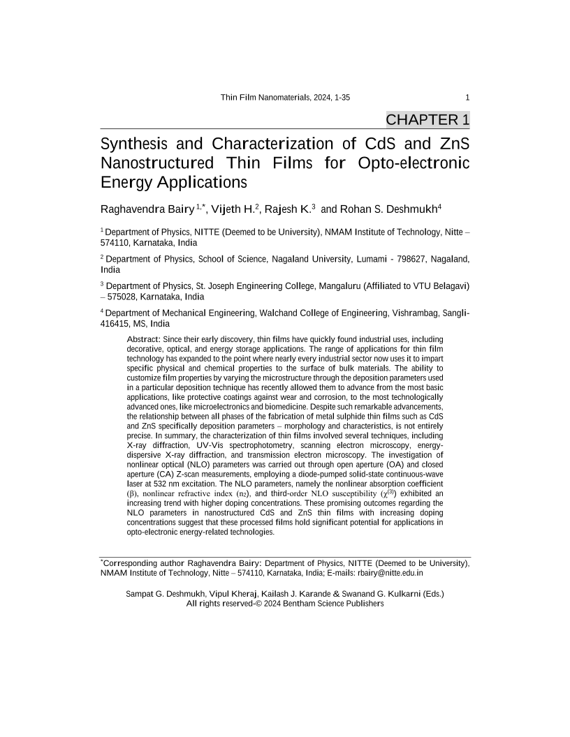
Since their early discovery, thin films have quickly found industrial uses, including decorative, optical, and energy storage applications. The range of applications for thin film technology has expanded to the point where nearly every industrial sector now uses it to impart specific physical and chemical properties to the surface of bulk materials. The ability to customize film properties by varying the microstructure through the deposition parameters used in a particular deposition technique has recently allowed them to advance from the most basic applications, like protective coatings against wear and corrosion, to the most technologically advanced ones, like microelectronics and biomedicine. Despite such remarkable advancements, the relationship between all phases of the fabrication of metal sulphide thin films such as CdS and ZnS specifically deposition parameters morphology and characteristics, is not entirely precise. In summary, the characterization of thin films involved several techniques, including X-ray diffraction, UV-Vis spectrophotometry, scanning electron microscopy, energydispersive X-ray diffraction, and transmission electron microscopy. The investigation of nonlinear optical (NLO) parameters was carried out through open aperture (OA) and closed aperture (CA) Z-scan measurements, employing a diode-pumped solid-state continuous-wave laser at 532 nm excitation. The NLO parameters, namely the nonlinear absorption coefficient (β), nonlinear refractive index (n2), and third-order NLO susceptibility (χ(3)) exhibited an increasing trend with higher doping concentrations. These promising outcomes regarding the NLO parameters in nanostructured CdS and ZnS thin films with increasing doping concentrations suggest that these processed films hold significant potential for applications in opto-electronic energy-related technologies.
-
From This Site
/content/books/9789815256086.chapter-1dcterms_subject,pub_keyword-contentType:Journal -contentType:Figure -contentType:Table -contentType:SupplementaryData105

