A Comprehensive Study on High Electron Mobility Transistors

- Authors: G. Purnachandra Rao1, Tanjim Rahman2, E Raghuveera3, Trupti Ranjan Lenka4
-
View Affiliations Hide Affiliations1 Department of Electronics and Communication Engineering, National Institute of Technology, Silchar 788010, Assam, India 2 Department of Electronics and Communication Engineering, National Institute of Technology, Silchar-788010, Assam, India 3 Department of Electronics and Communication Engineering, National Institute of Technology, Silchar-788010, Assam, India 4 Department of Electronics and Communication Engineering, National Institute of Technology, Silchar-788010, Assam, India
- Source: Nanoelectronic Devices and Applications , pp 115-129
- Publication Date: July 2024
- Language: English
A Comprehensive Study on High Electron Mobility Transistors, Page 1 of 1
< Previous page | Next page > /docserver/preview/fulltext/9789815238242/chapter-5-1.gif
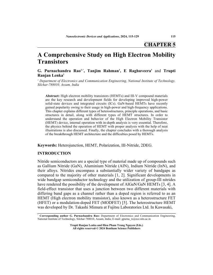
High electron mobility transistors (HEMTs) and III-V compound materials are the key research and development fields for developing improved high-power solid-state devices and integrated circuits (ICs). GaN-based HEMTs have recently gained popularity owing to their usage in high-power and high-frequency applications. This chapter explains different types of heterostructures, principle operations, and basic structures in detail, along with different types of HEMT structures. In order to understand the operation and behavior of the High Electron Mobility Transistor (HEMT) device, internal operation with in-depth analysis is very essential. Therefore, the physics behind the operation of HEMT with proper analysis with the help of neat illustrations is also discussed. Finally, the chapter concludes with a thorough analysis of the breakthrough HEMT architecture and the difficulties posed by HEMTs.
-
From This Site
/content/books/9789815238242.chapter-5dcterms_subject,pub_keyword-contentType:Journal -contentType:Figure -contentType:Table -contentType:SupplementaryData105

